Nanoscale surface patterns for advanced heat control
A nanofabrication technique 1,000 times faster opens the door to future thermal technologies
What the research is about
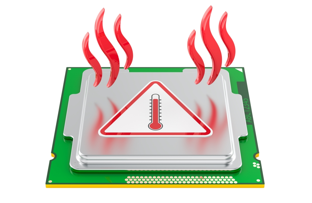
Think about how your smartphone becomes warm when you use it for a long time. Inside the chip, electrons move rapidly and collide with atoms. Each collision makes the atoms vibrate. These tiny vibrations are what we feel as heat.
Scientists call these vibrational waves phonons. Heat travels through materials as phonons move from place to place.
Phonons typically travel distances ranging from tens of nanometers (a nanometer is one billionth of a meter) to several micrometers. If we create structures on a material that match this scale, we can control how heat flows—making it harder for heat to pass through, or guiding it in specific directions. Over the past two decades, researchers have shown that nanometer-scale structures can finely tune heat transport in this way.
However, the biggest challenge has been how to fabricate such nanostructures efficiently. Conventional techniques such as electron-beam lithography can create extremely fine patterns, but they are too slow for large areas. Other conventional methods require multiple complex steps. While they demonstrated scientific possibilities in laboratories, they were not practical for large-scale, real-world applications.
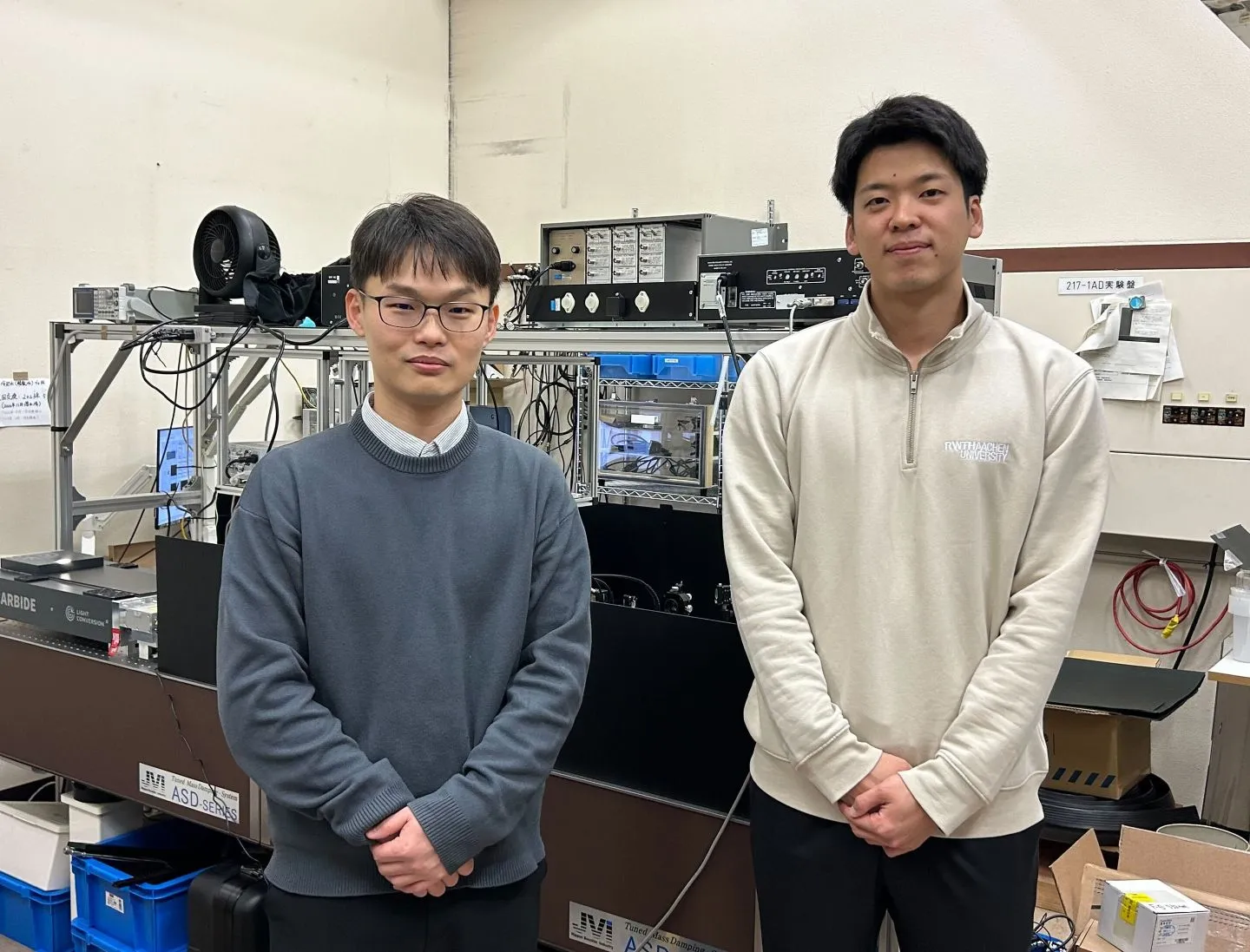
To overcome this barrier, a research team led by Assistant Professor Kim Byunggi and Professor Kazuyoshi Fushinobu of Institute of Science Tokyo (Science Tokyo), together with Professor Masahiro Nomura and colleagues at The University of Tokyo, focused on a special type of ultrafast laser called a femtosecond laser (a femtosecond is one quadrillionth of a second). They set out to develop a method that can directly imprint highly ordered nanostructures onto a material’s surface simply by shining the laser on it.
Why this matters
The team demonstrated that uniform nanostructures can be formed over centimeter-scale areas in a single step—without masks or chemical processes. Remarkably, the fabrication speed is more than 1,000 times faster than conventional electron-beam methods. This breakthrough significantly improves the feasibility of large-scale production.
But what does this mean in practice? The researchers applied the technique to a thin film of silicon, the fundamental material used in smartphone and computer chips. After forming the nanostructures, the material’s ability to conduct heat—known as its thermal conductivity—changed significantly. In untreated silicon, the thermal conductivity was 101 W/m·K. After nanostructuring, it decreased to 76 W/m·K, showing a clear suppression of heat flow.
At first glance, this may look like a simple numerical difference. In fact, it goes beyond what previous theoretical predictions had considered to be the lower limit for such thin films.
Why did this happen? The answer lies in the nanoscale patterns themselves. The periodic structures block phonons that attempt to travel long distances, while the fine surface roughness created by the laser further disrupts their motion. As a result, phonons cannot move freely, and the overall flow of heat is strongly reduced.
Achieving both high processing speed and precise thermal control was not easy. The team repeatedly refined fabrication conditions, building and testing prototypes until they established design guidelines that enable scalable production while enhancing heat-control performance.
What’s next
This technology has the potential to support the next generation of computing systems. For example, in quantum computers—where even tiny thermal fluctuations can affect performance—reducing unwanted heat is essential. The technique may also contribute to technologies that convert heat directly into electricity, as well as to thermal management in supercomputers and data centers that perform enormous amounts of calculations.
Importantly, this method is compatible with semiconductor manufacturing processes already used in today’s smartphones and computers. It may be applied without requiring entirely new fabrication infrastructure. In this way, an idea born in fundamental research could bridge the gap to real-world devices.
Comment from the researcher
Nanotechnology allows us to manipulate a world so small that it is barely visible even under a microscope—it challenges our imagination. To turn that imagination into technologies that benefit society, interdisciplinary approaches are essential.
In this research, we repurposed and advanced a fabrication method originally used in another field to make nanotechnology for heat control more practical. As electronic devices continue to evolve and energy challenges grow more serious, we hope to propose practical solutions that apply nanotechnology from multiple perspectives.
(Kim Byunggi, Assistant Professor, School of Engineering, Institute of Science Tokyo)
Dive deeper

Contact
Research Support Service Desk